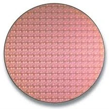
Silicon wafers disc
About[]
A wafer is a thin slice of semiconductor material, such as a silicon crystal, used in the fabrication of integrated circuit microchips, and other microdevices. The wafer serves as the substrate for microelectronic devices built in and over the wafer and undergoes many microfabrication process steps such as doping or ion implantation, etching, deposition of various materials, and photolithographic patterning.
Several types of solar cells are made from such wafers. A solar wafer is a circular solar cell made from the entire wafer rather than cutting into smaller rectangular solar cells.
Standard Sizes[]
Silicon wafers are available in a variety of sizes from 25.4 mm (1 inch) to 300 mm (11.8 inches).[8] Semiconductor fabrication plants (also known as fabs) are defined by the size of wafers that they are tooled to produce. The size has gradually increased to improve throughput and reduce cost with the current state-of-the-art fab considered to be 300mm (12 inch), with the next standard projected to be 450mm (18 inch). Intel, TSMC and Samsung are separately conducting research to the advent of 450mm "prototype" (research) fabs by 2012, though serious hurdles remain.
Reference[]