Junction Field Effect Transistor
The field-effect transistor (FET) is a type of transistor that relies on an electric field to control the shape and hence the conductivity of a channel of one type of charge carrier in a semiconductor material. FETs are sometimes called unipolar transistors to contrast their single-carrier-type operation with the dual-carrier-type operation of Bipolar Junction Transistors (BJT). The concept of the FET predates the BJT, though it was not physically implemented until after BJTs due to the limitations of semiconductor materials and relative ease of manufacturing BJTs compared to FETs at the time.
History[]
Field-effect transistors were invented by Julius Edgar Lilienfeld in 1925 and by Oskar Heil in 1934, but practical devices were not made until much later.
Terminals[]
All FETs have a gate, drain, and source terminal that are roughly similar to the base, collector, and emitter of BJTs. Aside from the JFET, all FETs also have a fourth terminal called the body, base, bulk, or substrate. This fourth terminal serves the technical purpose of biasing the transistor into operation; it is rare to make non-trivial use of the body terminal in circuit designs, but its presence is important when setting up the integrated circuit layout of an integrated circuit.
The names of the terminals refer to their functions. The gate terminal may be thought of as controlling the opening and closing of a physical gate. This gate permits electrons to flow through or blocks their passage by creating or eliminating a channel between the source and drain. Electrons flow from the source terminal towards the drain terminal if influenced by an applied voltage. The body simply refers to the bulk of the semiconductor in which the gate, source and drain lie. Usually the body terminal is connected to the highest or lowest voltage within the circuit, depending on type. The body terminal and the source terminal are sometimes connected together since the source is also sometimes connected to the highest or lowest voltage within the circuit, however there are several uses of FETs which do not have such a configuration, such as transmission gates and cascode circuits.
Composition[]
The FET can be constructed from a number of semiconductors, silicon being by far the most common. Most FETs are made with conventional bulk semiconductor processing techniques, using the single crystal semiconductor wafer as the active region, or channel.
Among the more unusual body materials are amorphous silicon, polycrystalline silicon or other amorphous semiconductors in thin-film transistors or organic field effect transistors that are based on organic semiconductors and often apply organic gate insulators and electrodes.
Types of field-effect transistors[]
The channel of a FET (explained below) is Doping (semiconductor) to produce either an N-type semiconductor or a P-type semiconductor. The drain and source may be doped of opposite type to the channel, in the case of enhancement mode FETs, or doped of similar type to the channel as in depletion mode FETs. Field-effect transistors are also distinguished by the method of insulation between channel and gate. Types of FETs are:
- The MOSFET (Metal–Oxide–Semiconductor Field-Effect Transistor) utilizes an insulator (typically silicon dioxide) between the gate and the body .
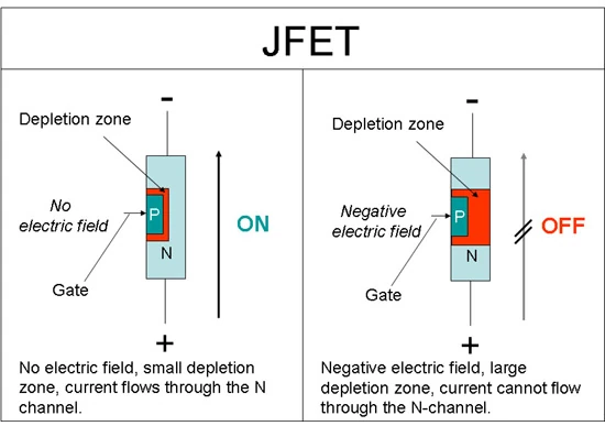
- The JFET (Junction Field-Effect Transistor) uses a reverse biased p-n junction to separate the gate from the body.
- The MESFET (Metal–Semiconductor Field-Effect Transistor) substitutes the p-n junction of the JFET with a Schottky barrier; used in GaAs and other III-V semiconductor materials.
- Using bandgap engineering in a ternary semiconductor like AlGaAs gives a HEMT (High Electron Mobility Transistor), also called an HFET (heterostructure FET). The fully depleted wide-band-gap material forms the isolation between gate and body.
- The MODFET (Modulation-Doped Field Effect Transistor) uses a quantum well structure formed by graded doping of the active region.
- The IGBT (Insulated-Gate Bipolar Transistor) is a device for power control. It has a structure akin to a MOSFET coupled with a bipolar-like main conduction channel. These are commonly used for the 200-3000 V drain-to-source voltage range of operation. Power MOSFETs are still the device of choice for drain-to-source voltages of 1 to 200 V.
- The FREDFET (Fast Reverse or Fast Recovery Epitaxial Diode FET) is a specialized FET designed to provide a very fast recovery (turn-off) of the body diode.
- The ISFET is an Ion-Sensitive Field Effect Transistor used to measure ion concentrations in a solution; when the ion concentration (such as pH) changes, the current through the transistor will change accordingly.
- The DNA field-effect transistor (DNAFET) is a specialized FET that acts as a biosensor, by using a gate made of single-strand DNA molecules to detect matching DNA strands.
FET operation[]
The FET controls the flow of electrons (or electron holes) from the source to drain by affecting the size and shape of a "conductive channel" created and influenced by voltage (or lack of voltage) applied across the gate and source terminals. (For ease of discussion, this assumes body and source are connected). This conductive channel is the "stream" through which electrons flow from source to drain.
Consider an n-channel "depletion-mode" device. A negative gate-to-source voltage causes a depletion region to expand in width and encroach on the channel from the sides, narrowing the channel. If the depletion region expands to completely close the channel, the resistance of the channel from source to drain becomes large, and the FET is effectively turned off like a switch. Likewise a positive gate-to-source voltage increases the channel size and allows electrons to flow easily.
Now consider an n-channel "enhancement-mode" device. A positive gate-to-source voltage is necessary to create a conductive channel, since one does not exist naturally within the transistor. The positive voltage attracts free-floating electrons within the body towards the gate, forming a conductive channel. But first, enough electrons must be attracted near the gate to counter the dopant ions added to the body of the FET; this forms a region free of mobile carriers called a depletion region, and the phenomenon is referred to as the threshold voltage of the FET. Further gate-to-source voltage increase will attract even more electrons towards the gate which are able to create a conductive channel from source to drain; this process is called inversion.
For either enhancement- or depletion-mode devices, at drain-to-source voltages much less than gate-to-source voltages, changing the gate voltage will alter the channel resistance, and drain current will be proportional to drain voltage (referenced to source voltage). In this mode the FET operates like a variable resistor and the FET is said to be operating in a linear mode or ohmic mode.
If drain-to-source voltage is increased, this creates a significant asymmetrical change in the shape of the channel due to a gradient of voltage potential from source to drain. The shape of the inversion region becomes "pinched-off" near the drain end of the channel. If drain-to-source voltage is increased further, the pinch-off point of the channel begins to move away from the drain towards the source. The FET is said to be in saturation mode.
The saturation mode, or the region between ohmic and saturation, is used when amplification is needed. The in-between region is sometimes considered to be part of the ohmic or linear region, even where drain current is not approximately linear with drain voltage.
Even though the conductive channel formed by gate-to-source voltage no longer connects source to drain during saturation mode, charge carriers are not blocked from flowing. Considering again an n-channel device, a depletion region exists in the p-type body, surrounding the conductive channel and drain and source regions. The electrons which comprise the channel are free to move out of the channel through the depletion region if attracted to the drain by drain-to-source voltage. The depletion region is free of carriers and has a resistance similar to silicon. Any increase of the drain-to-source voltage will increase the distance from drain to the pinch-off point, increasing resistance due to the depletion region proportionally to the applied drain-to-source voltage. This proportional change causes the drain-to-source current to remain relatively fixed independent of changes to the drain-to-source voltage and quite unlike the linear mode operation. Thus in saturation mode, the FET behaves as a current source rather than as a resistor and can be used most effectively as a voltage amplifier. In this case, the gate-to-source voltage determines the level of constant current through the channel.
Uses[]
The most commonly used FET is the MOSFET. The CMOS (complementary-symmetry metal oxide semiconductor) process technology is the basis for modern digital integrated circuits. This process technology uses an arrangement where the (usually "enhancement-mode") p-channel MOSFET and n-channel MOSFET are connected in series such that when one is on, the other is off.
The fragile insulating layer of the MOSFET between the gate and channel makes it vulnerable to electrostatic discharge during handling. This is not usually a problem after the device has been installed in a properly designed circuit.
In FETs electrons can flow in either direction through the channel when operated in the linear mode, and the naming convention of drain terminal and source terminal is somewhat arbitrary, as the devices are typically (but not always) built symmetrically from source to drain. This makes FETs suitable for switching analog signals between paths (multiplexing). With this concept, one can construct a solid-state mixing board, for example.
External links[]
- PBS The Field Effect Transistor
- Junction Field Effect Transistor
- The Enhancement Mode MOSFET
- CMOS gate circuitry
- Winning the Battle Against Latchup in CMOS Switches
- Nanotube FETs at IBM Research
- Field Effect Transistors in Theory and Practice
Video[]
thumb|300px|right